Image:Wafertraksystem.jpg
From Wikipedia, the free encyclopedia
Size of this preview: 800 × 600 pixels
Full resolution (2,048 × 1,536 pixels, file size: 577 KB, MIME type: image/jpeg)
| | This is a file from the Wikimedia Commons. The description on its description page there is shown below.
|
[edit] Summary
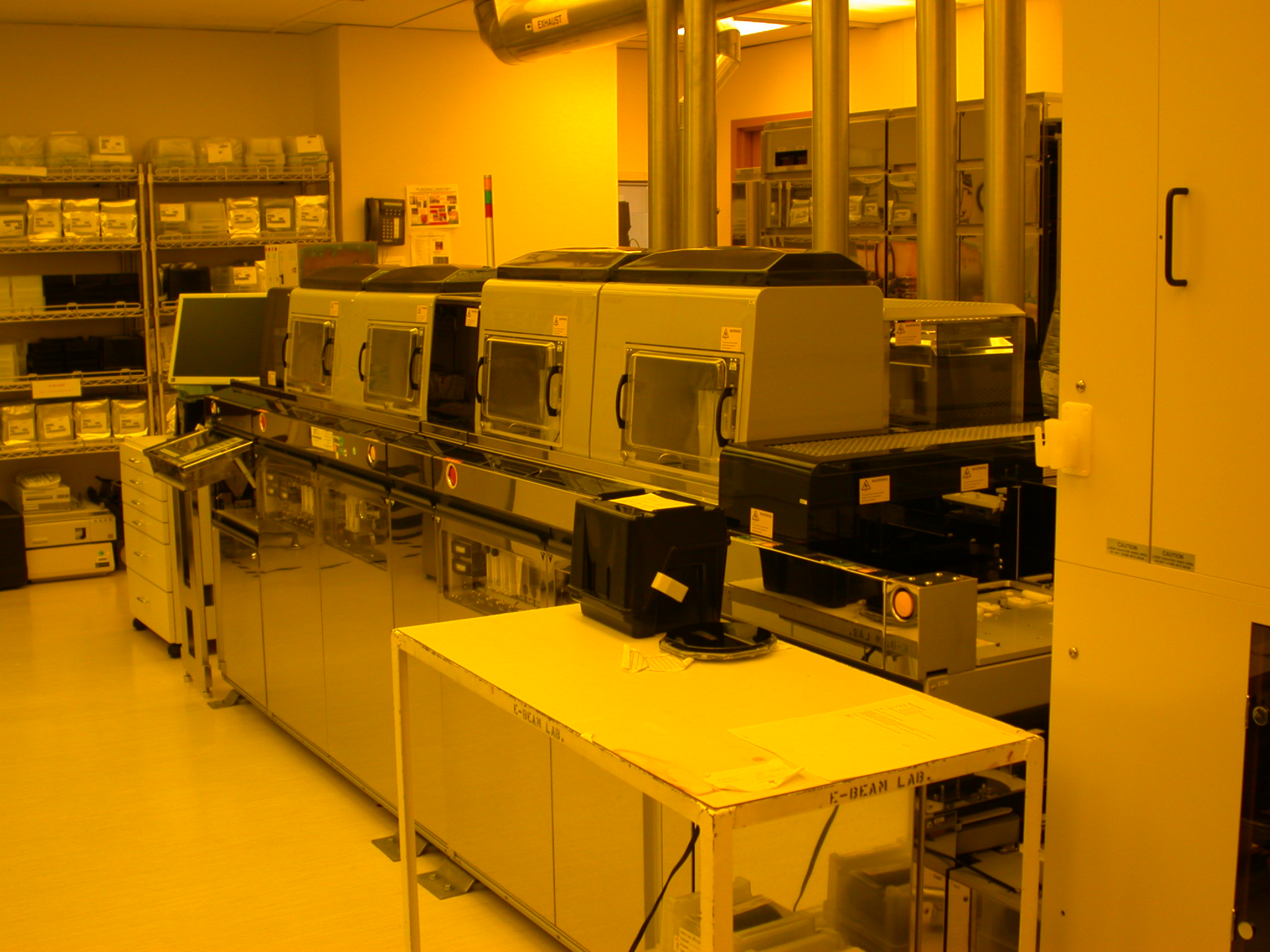
An aligner is a major piece of equipment used in semiconductor device fabrication. Trending from upper left to lower right is the wafer-track system of a photolithographic aligner that uses the "i-line" from a mercury arc lamp (wavelength 365 nm) to expose photoresist deposited on silicon wafers. Wafers are robotically loaded from a carrier at the left hand of the system and progressively are coated with photoresist, exposed to ultraviolet light, and "developed". The development step involves using a solvent to remove either the exposed (positive photoresist) or unexposed (negative photoresist) portions of the film. In the foreground is a black plastic box containing silicon wafers with a diameter of 6" (125 mm).
Photo taken at HP Labs by Alison Chaiken using a Nikon 995 camera. Note that the light in the room really is yellow!
[edit] Licensing

File history
Click on a date/time to view the file as it appeared at that time.
| Date/Time | Dimensions | User | Comment | |
|---|---|---|---|---|
| current | 02:11, 3 February 2006 | 2,048×1,536 (577 KB) | Chaiken | (An '''aligner''' is a major piece of equipment used in semiconductor device fabrication.Trending from upper left to lower right is the wafer-track system of a photolithographic aligner that us) |
File links
Metadata
This file contains additional information, probably added from the digital camera or scanner used to create or digitize it. If the file has been modified from its original state, some details may not fully reflect the modified file.
| Camera manufacturer | NIKON |
|---|---|
| Camera model | E995 |
| Exposure time | 2/55 sec (0.036363636363636) |
| F-number | f/2.7 |
| Date and time of data generation | 21:05, 31 January 2006 |
| Lens focal length | 8.9 mm |
| Orientation | Normal |
| Horizontal resolution | 300 dpi |
| Vertical resolution | 300 dpi |
| Software used | E995v1.7 |
| File change date and time | 21:05, 31 January 2006 |
| Y and C positioning | 2 |
| Exposure Program | Normal program |
| ISO speed rating | 100 |
| Exif version | 2.1 |
| Date and time of digitizing | 21:05, 31 January 2006 |
| Image compression mode | 2 |
| Exposure bias | 0 |
| Maximum land aperture | 2.8 |
| Metering mode | Pattern |
| Light source | Unknown |
| Flash | 0 |
| Color space | sRGB |

